I recently bought an Alinco DJ-G7 handheld radio. After playing for several days with it, I went on a holiday trip. I did not take the drop-in charger with me cause of its size. When the battery was exhausted, I tried to charge it through DC connector at the right side of the DJ-G7. After plugging the DC connector, no message appeared on the screen. After checking that the right battery type was set in the configuration I did several desperate full resets. I concluded that there should be a failure inside the unit. I even checked my DJ-G7 against a friend's charger with no luck. Something should be wrong inside the unit.
I emailed the supplier who sold me the DJ-G7 and told me that I should send the DJ-G7 to the technical service. Several friends convinced me to do the repair on my own. I did not know how long I will be appart from my DJ-G7, it could be months, and what is worse, what they were going to do to fix it. I thank them for pointing me in that direction, it was the right one.
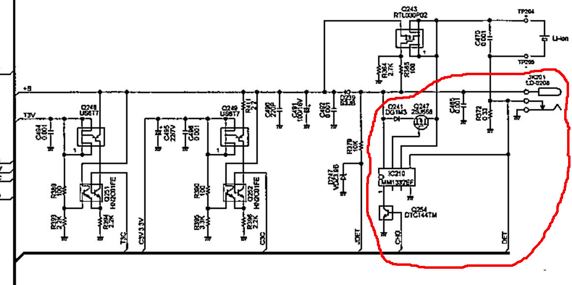
After studying service manual schematic I found the probable place for the fault. Sorry but the quality of the picture is very bad but it is the quality of the service manual as supplied by Alinco in its WEB page:
The handheld was working ok so voltage regulators Q248 and Q249 should be ok. It also worked fine from the battery so Q243 bypass should be ok. The failure might be inside the red circle. I also suspected from the DC connector internal switch. I checked it using my resistance meter. 0.33 ohm resistance appeared from negative battery terminal to GND chassis when DC plug was interted.
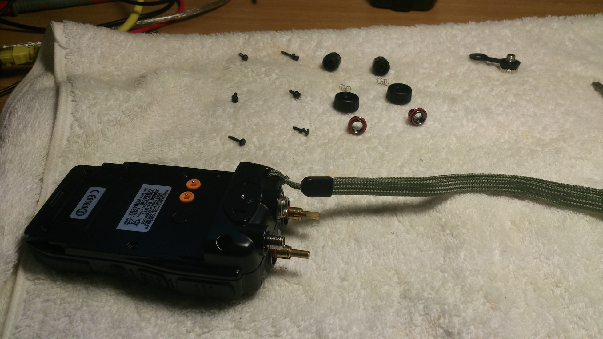
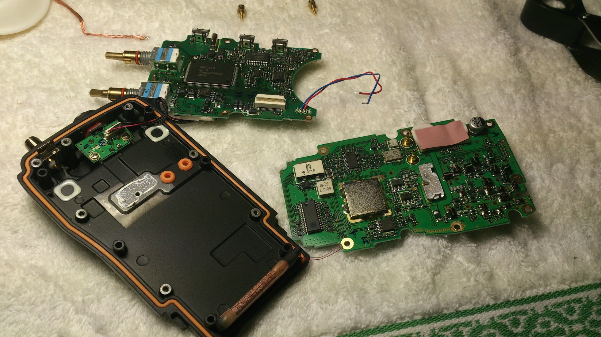
I must admit that I was terrified of disassembling the unit. It was my first handheld dissassembly and from the begining I found difficulties that made me think twice about abandoning the repair. Everything is so small.... Pictures speak by themselves so will describe only the difficult stages or things worth mentioning.
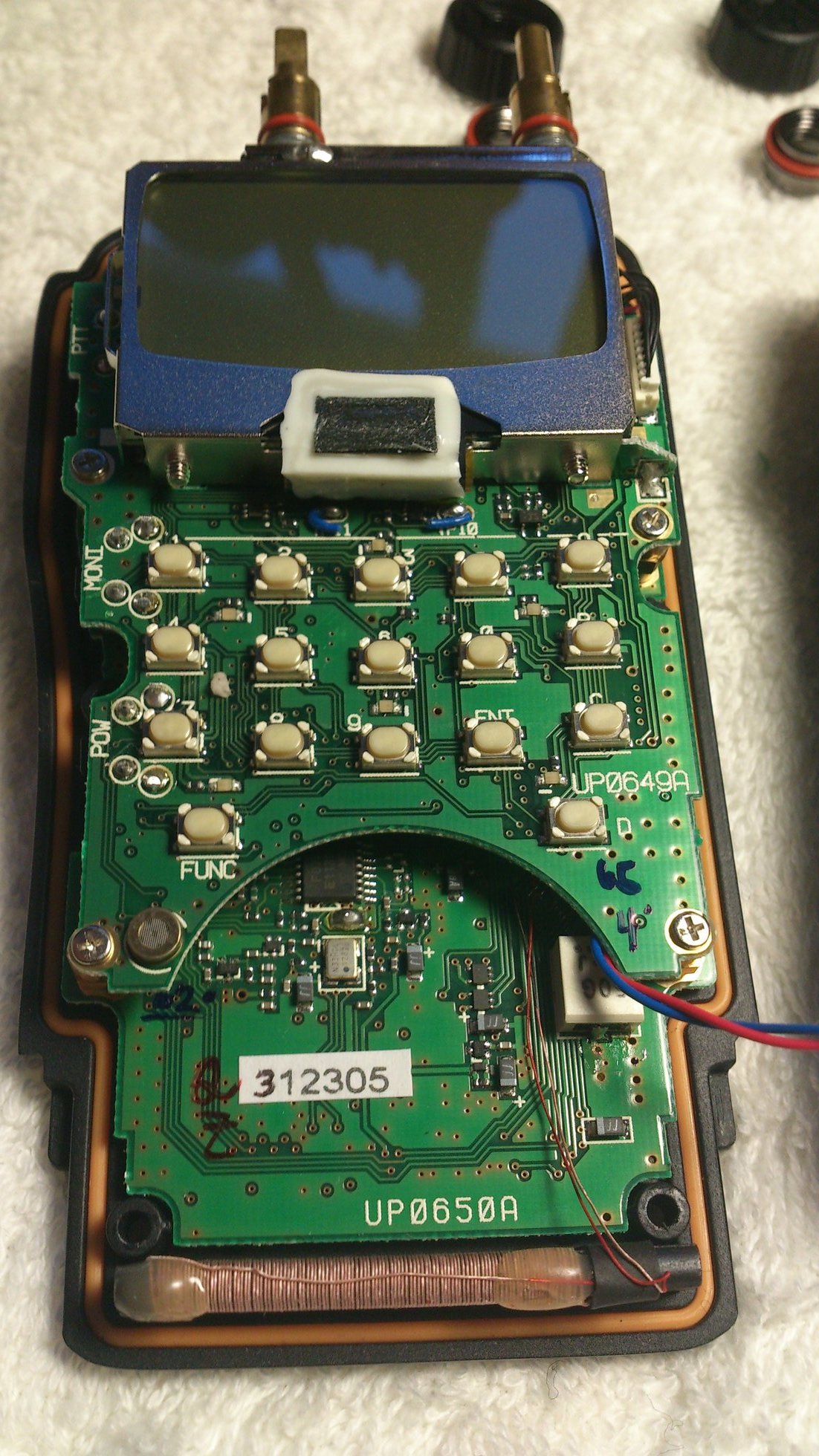
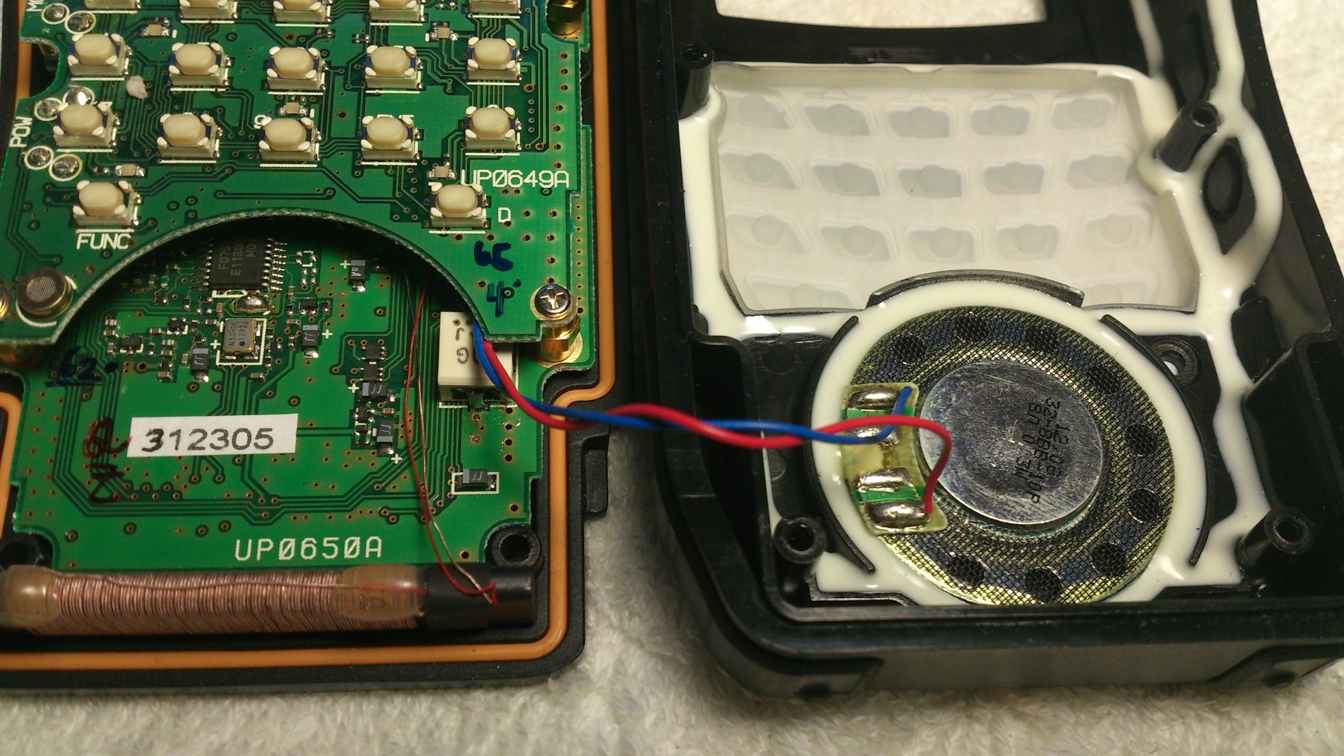
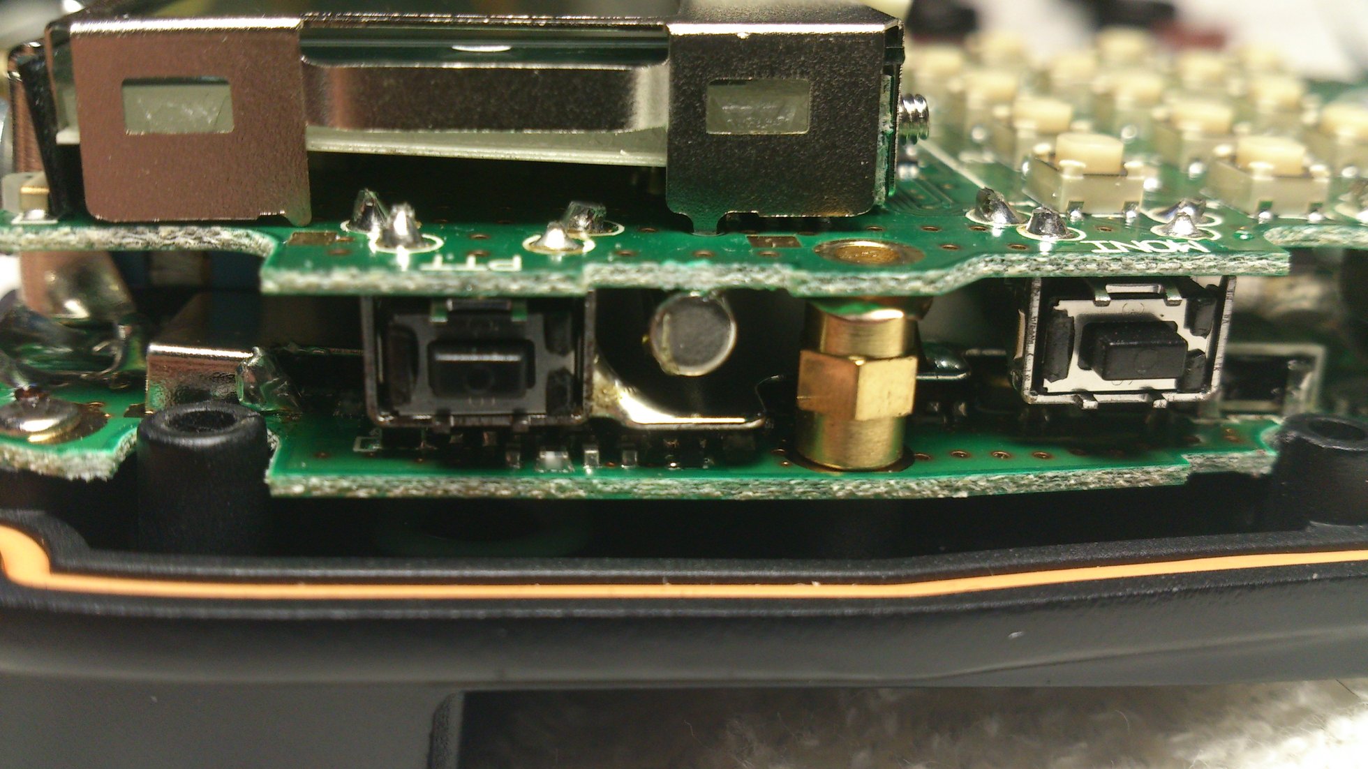
To remove CPU Unit PCB, first remove PTT solder to the shielding metal. Use desoldering braid, flux and a soldering iron. Be careful, do not drop any soldering material below. A little cable that shorts display frame to a metal plate that holds the main and sub dials should also be removed. This can be done with care using a soldering iron and pliers. Do not forget to solder those two points when you assemble the unit again.
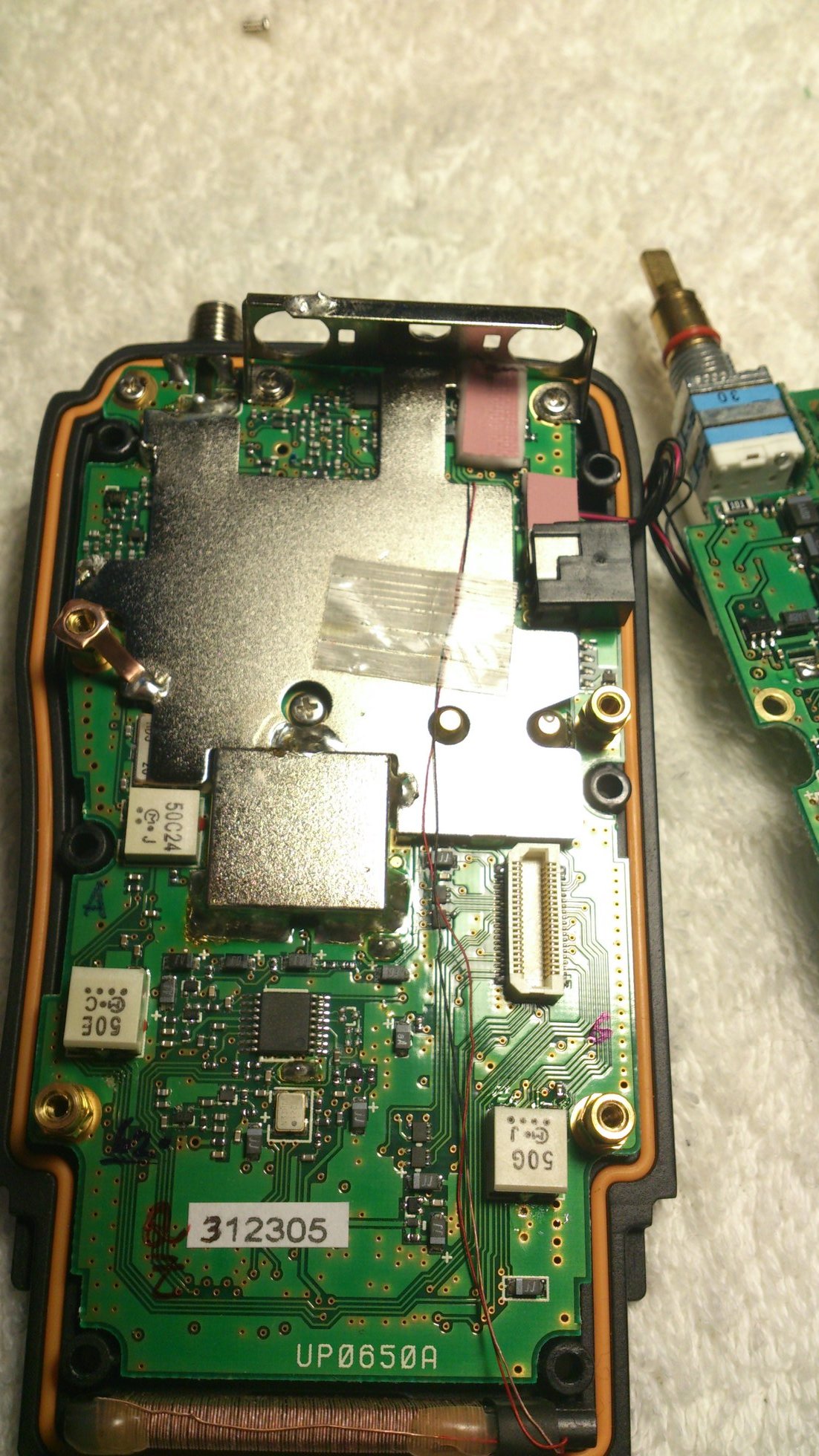
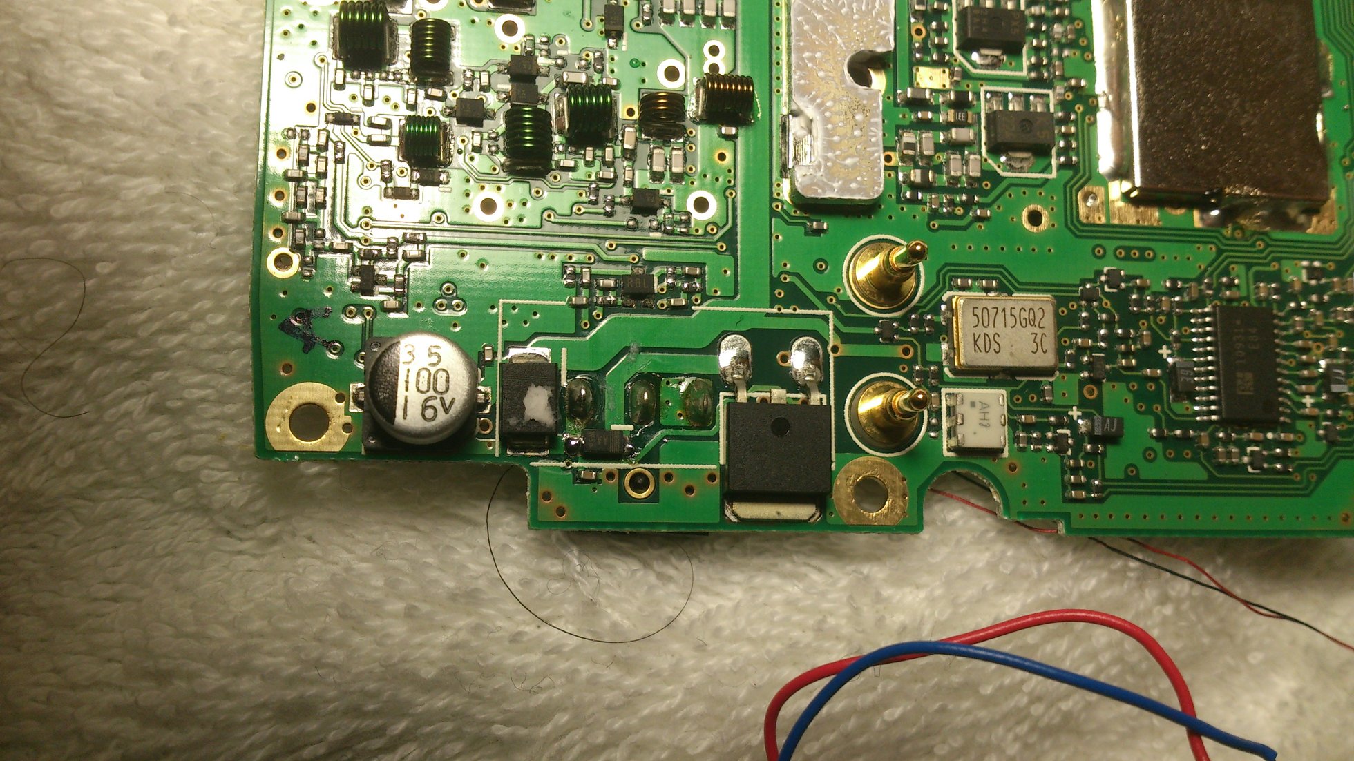
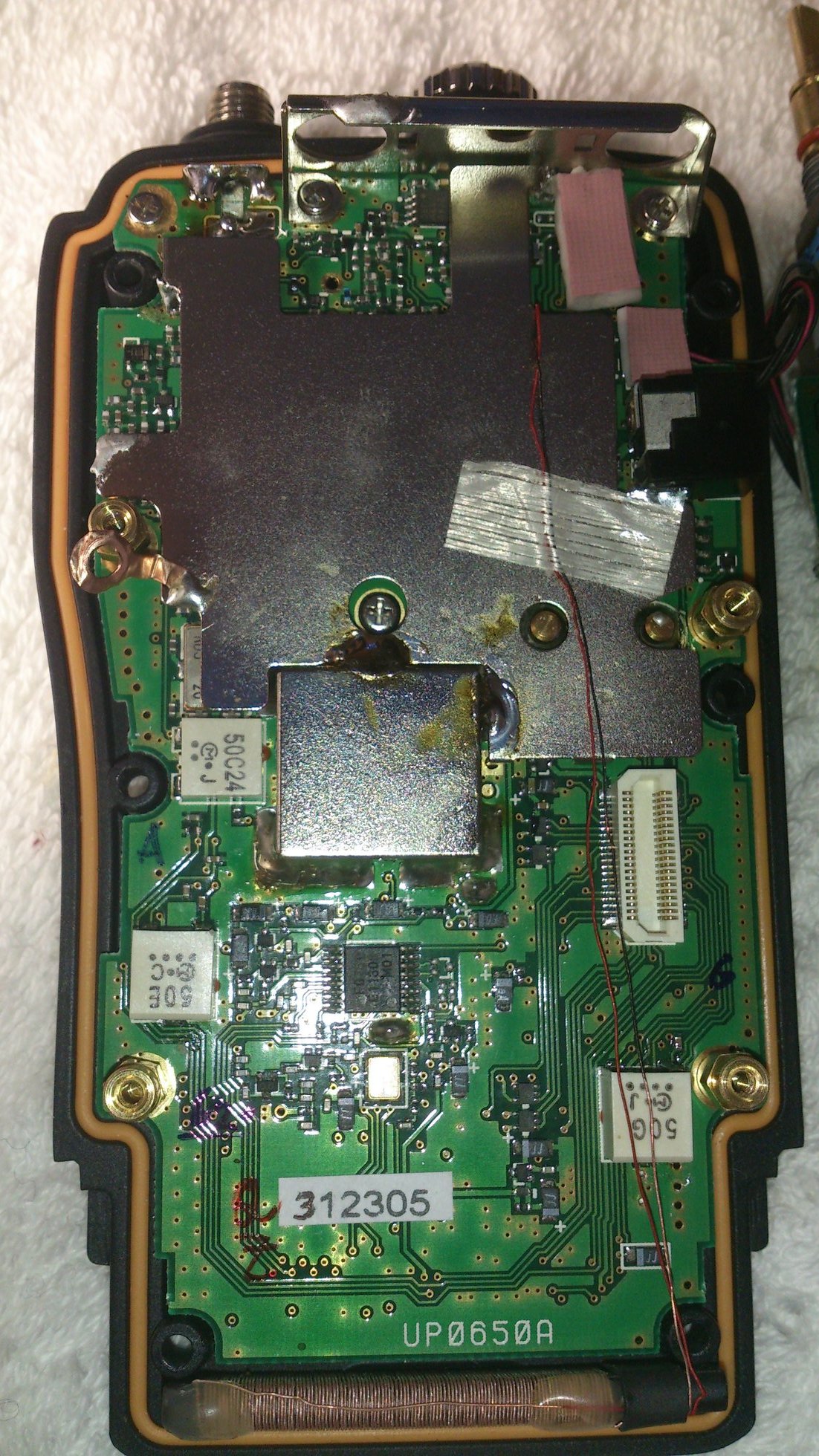
I found a horrible shielding plate soldered at four points to the Main Unit PCB. There is charging circuitry at both sides of PCB. At top side there are several components below the shielding plate, so I needed to remove the plate to see what was going on. Remove all solder at the four points using desoldering braid, flux and a soldering iron as before. Be careful with the bar antenna cables, they are thin and fragile, do not be fooled by the camera magnification . Remove the adhesive tape that holds them before applying heat. Metal plate dissipate heat quickly so you need a powerful soldering iron. I used my gas powered soldering iron.
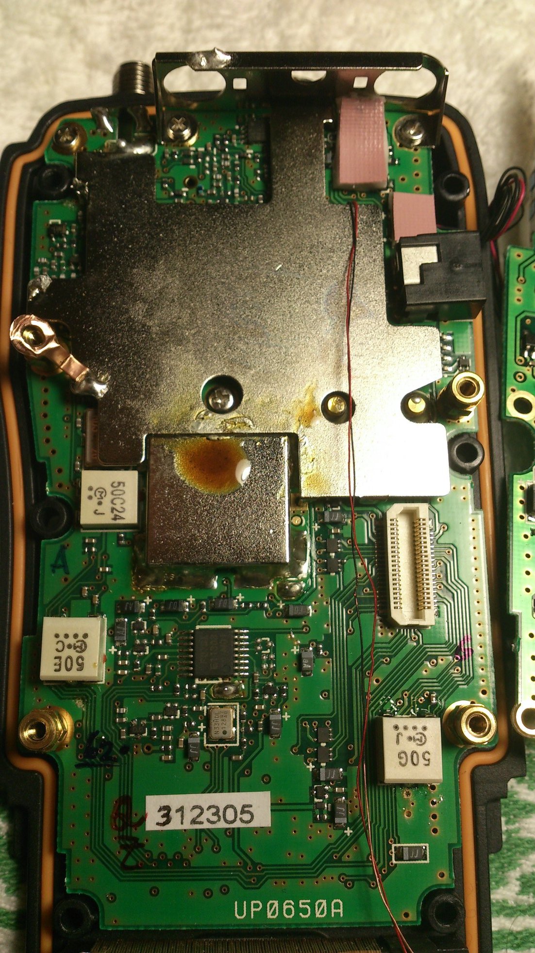
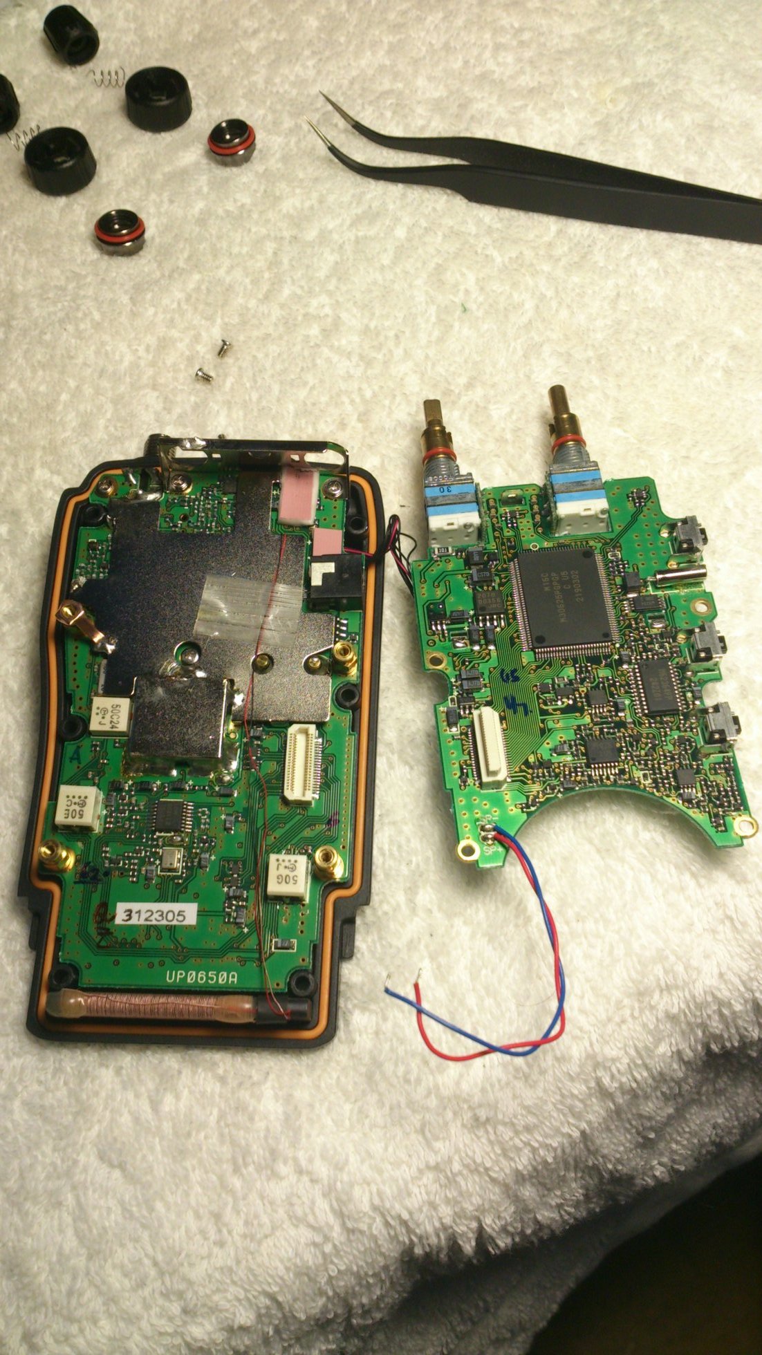
Before removing Main Unit PCB, desolder antenna connector inner an outer terminals
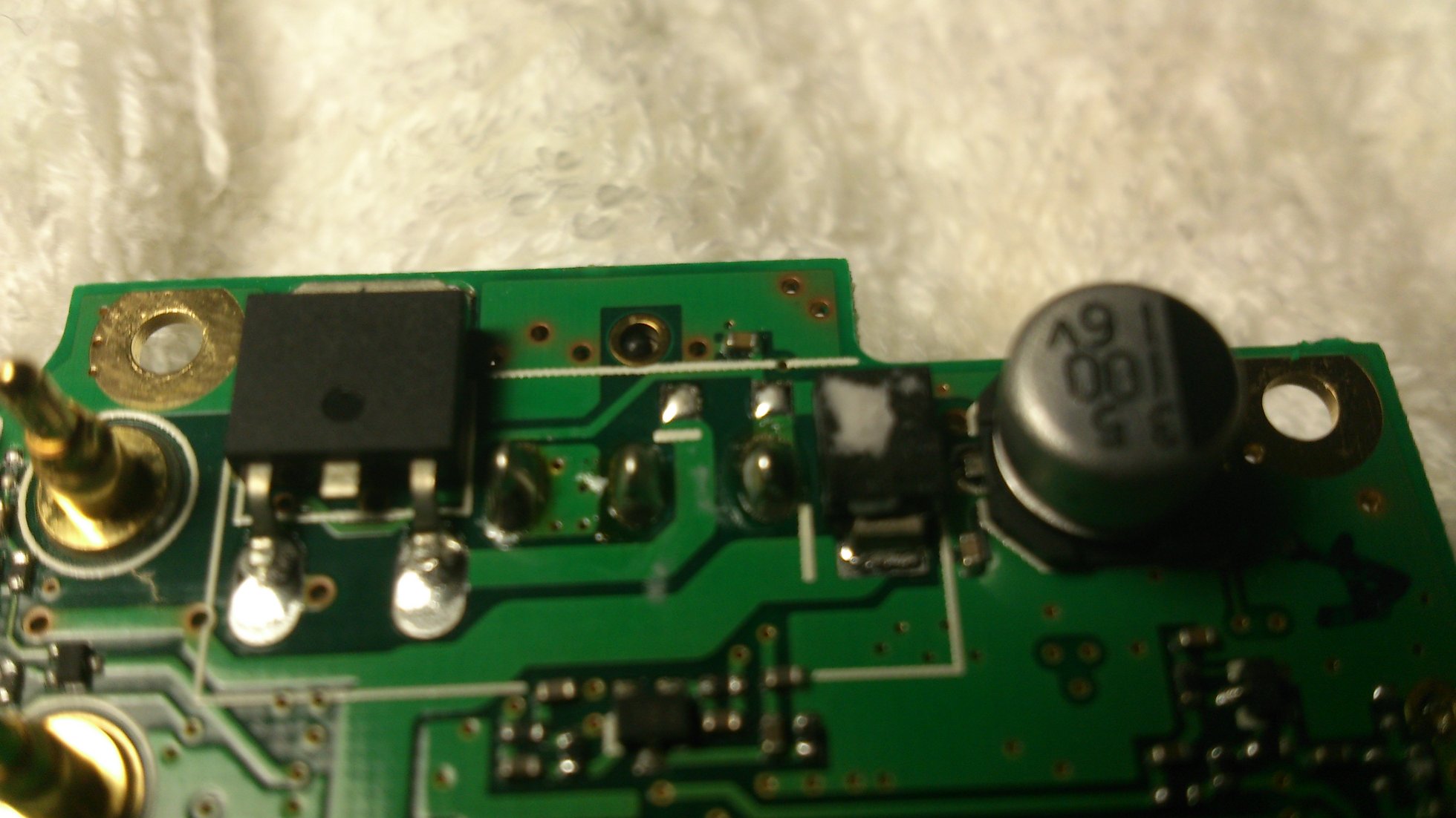
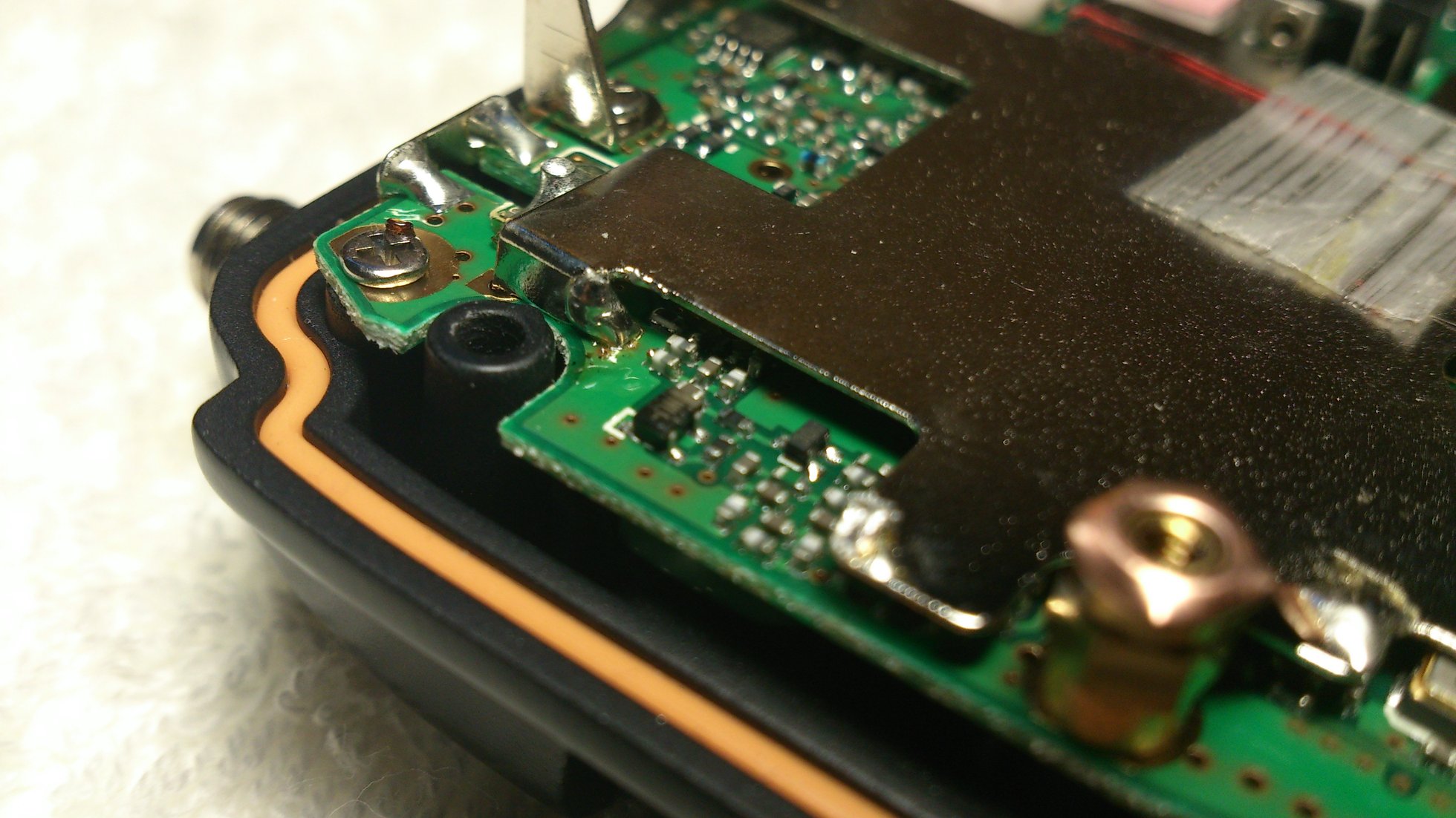
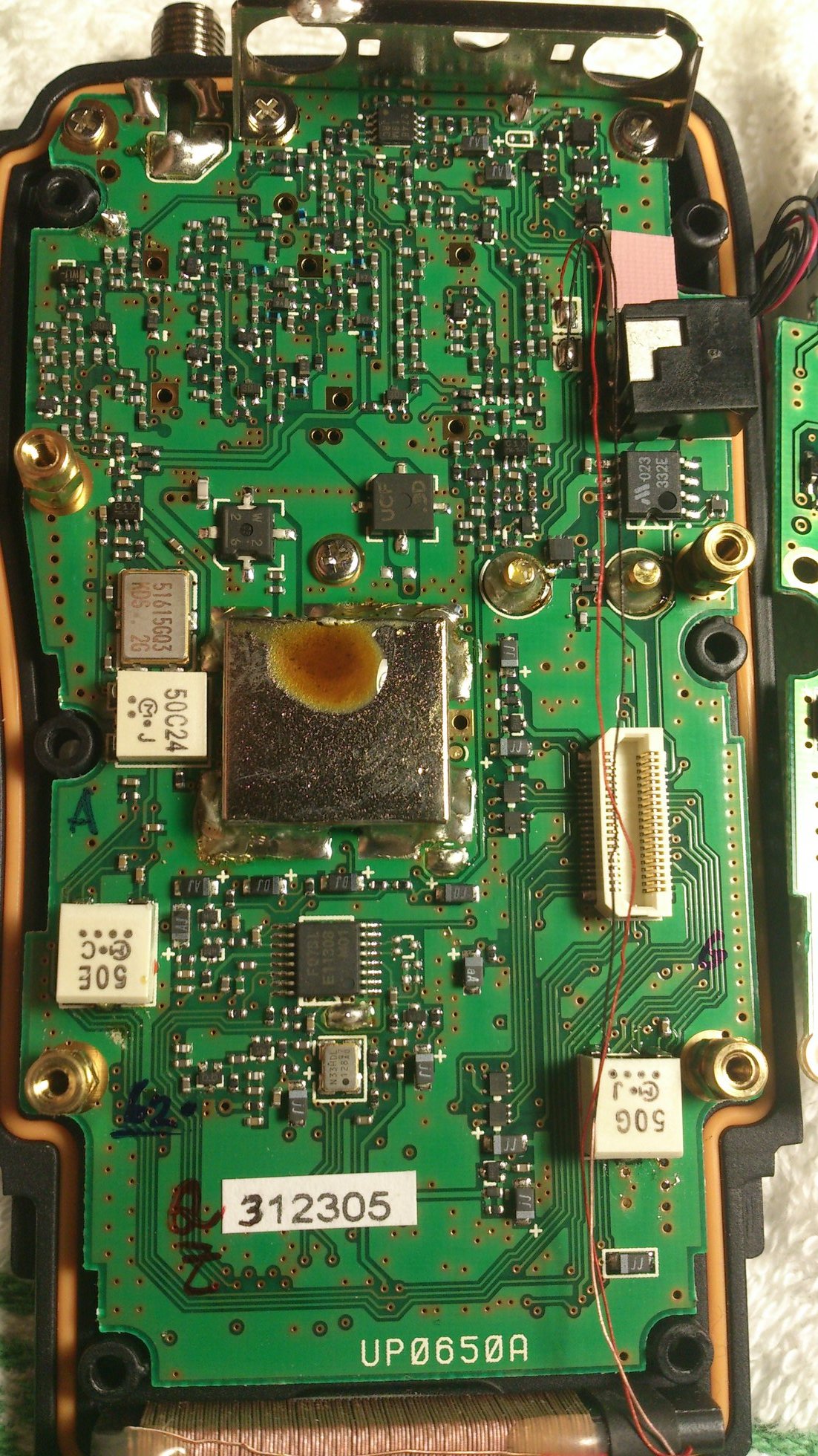
After removing the pink adhesive rubber tape over the charging parts, I soon found the reason of the malfunctioning: a missing diode. This is unbelievable, Q241 schottky diode was missing. I ordered a replacement diode with the help of Carlos, EB4FBZ, that quickly found a good substitute: a 1A, 30V, SOD-123F NXP PMEG3010EH schottky diode.
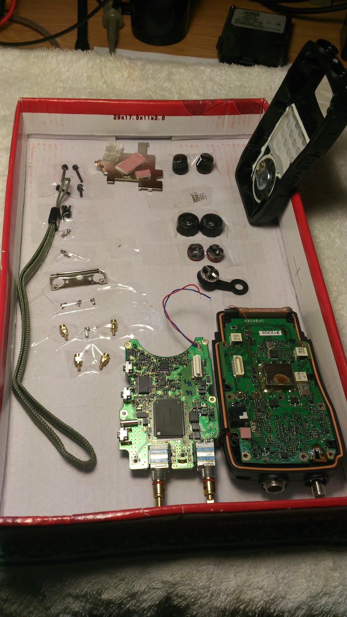
I placed all the parts fixed with adhesive tape over a shoe box cover. I waited during loooong 11 days until finally received the desired diode. I soldered it in place, I was really excited to see the result.
I put Main Unit PCB in place, soldered antenna connector terminals and soldered the plate carefully in four points, taking care that battery terminals were centered inside the plate holes. Do not forget to place the copper sheet that connects the shielding plate to one of the screws that support CPU Unit PCB:
I assembled everything carefully and could not wait for placing main and sub dial knobs, I inserted the DC plug:
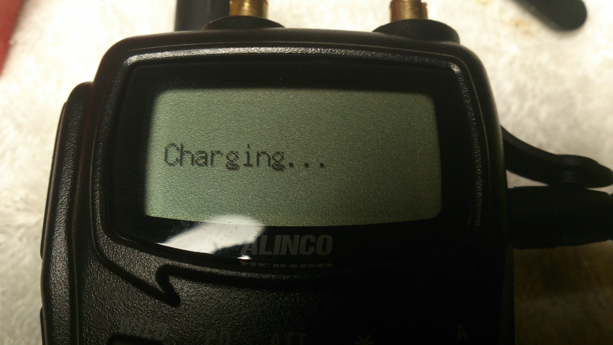
That's it! It works!
ALINCO DJ-G7/T/E SERVICE MANUAL
  Copyright (c)  2013 Ramiro Aceves .
  Permission is granted to copy, distribute and/or modify this document
  under the terms of the GNU Free Documentation License, Version 1.2
  or any later version published by the Free Software Foundation;
  with no Invariant Sections, no Front-Cover Texts, and no Back-Cover
  Texts.  A copy of the license is included in the section entitled "GNU
  Free Documentation License".